Copper is the most extensively used material mostly in the electrical & electronics sectors due to its superior thermal, and electrical conducting, high reflectivity and malleable properties of other materials. Applications range from heat exchanges, electrical conducting circuits, radio frequency equipment, heat sinks etc. However, these fundamental properties also acted as roadblocks to the development of copper additive manufacturing. But over a period of time, these challenges are overcome due to advancements in technologies and the immense benefit offered by copper as an AM material. The copper AM technology could create highly complex geometries, which are impossible to get by conventional manufacturing technologies. Today, copper-printed heat sinks keep electronic systems cool, rocket nozzles send space crafts into space, and high-efficiency RF equipment & copper AM-printed electricity conducting coils enhance the motor output. Various copper AM technologies are available, such as FDM, SLM, binder jetting and cold spray. We’ll be discussing all these technologies in this article.
SLM (Selective laser sintering)
SLM is the powder-based 3D printing process in which the raw metal powder is melted by the application of a high-intensity laser and fused together layer by layer over a built platform to create an object. As the platform moves down a new layer of powder metal is spread across the platform for the creation of the next layer. The entire process repeats over again and again unravelling the whole object. Copper is difficult to print via this method due to its high thermal conductivity and reflectivity. A recent development by Germany-based AM machines maker Trumpf of the green laser led to the fabrication of copper parts overcoming the challenges due to copper properties. This critical development opens the doors to the cost-effective development of copper parts in less time. Post-processing includes wire cutting, heat treatment, manual support removal etc.

3D-printed copper parts on a built plate. Image credits: GH Induction
FDM (Fused Deposition Modeling)
Perhaps the most cost-effective method of creating copper parts than any other technology available. In this process, the copper particles are mixed with the plastic filament and the same filament is extruded and deposited on the build platform in a Cartesian format just like any other FDM/FFF machine. However, the nozzle design and other specifications differ slightly from regular desktop FDM/FFF machines. Markforged is the pioneer in this field and has created the industrial FDM/FFF machine which can print many other metal parts along with copper. On the cost front, FDM/FFF-created parts cost almost one-third the price of SLM or other powder bed-based machines. Postprint operations include heat treatment and support removal.
Binder Jetting
Binder jetting is the process of creating a 3D printed part by depositing a binding liquid agent over the copper powder just like an inkjet paper printer followed by exposure to UV light to strengthen the binding bond between the copper particles. This process is comparatively fast, thermal free and does not require supporting structures for the overhang features. The 3D printed part is later sintered in a furnace to achieve the final desired component. Large complex geometries could be created in less time, costs less and lesser manual interventions are needed.
Cold Spray
In this process, softer metal powder(copper, aluminum) particles are blown thru a nozzle at supersonic speeds towards the target surface or a substrate. The high-impact force deforms the powder particles and fuses them together creating a layer. The process repeats layer by layer creating the desired object. The spraying nozzle is moved either in cartesian or multi-axis planes as per programming. This process is useful in creating larger geometric which are beyond the capabilities of powder bed fusion & binder jetting etc. Formed parts are later CNC machined to precise tolerances as per the design requirements. Large aerospace structures, fuel tanks, rocket nozzles and molds can be formed in less time and cost-effectively by this process.
Photopolymerization
3D printing by photopolymerization is usually known as stereolithography (SLA). Photopolymerization can produce parts with details and dimensions ranging from the micrometre- to meter scales and serves a variety of applications such as short-run tooling, presentation models, dental models, hearing aids, etc. However, a startup Holo has created a propriety DLP machine which high-resolution copper parts from the liquid resin or copper slurry. The formed part is later heat treated in a furnace before application. As per the company's claims, their set-up could produce resolutions up to 50 microns.

DLP made copper part. Image credits: Holo
Lamination
In this process, thin metal sheets are welded together sheet by sheet layer and simultaneously machining or post-process machining to get the desired geometry. Welding happens by the combination of high-frequency vibration and pressure applied over the copper sheets fusing together to create the part. This process is compatible with metals like copper, aluminum and copper aluminum together etc. Components like heat exchangers, heat sinks or embedded circuits could be created with this process which is unachievable by other AM processes.

Lamination process. Image credits: Loughborough University
Lamination process.
Key applications
- Electronics – The sector going to reap the maximum benefits out of the copper AM. The efficient and compact size of conductive elements like compact heat sinks for high-performance heat exchangers.
- Aerospace – Space crafts nozzles and combustion chambers for enhanced performance. Also, copper AM could create topology optimized low weight components which is essential for aerospace applications.
- Heat exchangers & sinks – Due to their high thermal conductivity, copper is the best material for demanding applications where a high rate of heat dissipation is required.
- RF antennas – Complex design, compact size and high-efficiency RF components could be created by copper AM.
- Electromagnetic coils – Electromagnetic induction coils are used for generating heat in a furnace or directly heating the metal for post-heating operations such as bending or shape forming. Complex coil shapes could be created for applications which are not possible to create by conventional manufacturing methods such as CNC, sheet metal etc.

Copper 3D printed rocket engine core. Image credits: LAUNCHER

3D printed copper bull horn antenna. Image credits: Markforged(Digital Metal)

3D printed copper heat exchanger. Image credits: FABRIC8LABS

Copper AM induction coil. Image credits: GH Induction
Conclusion
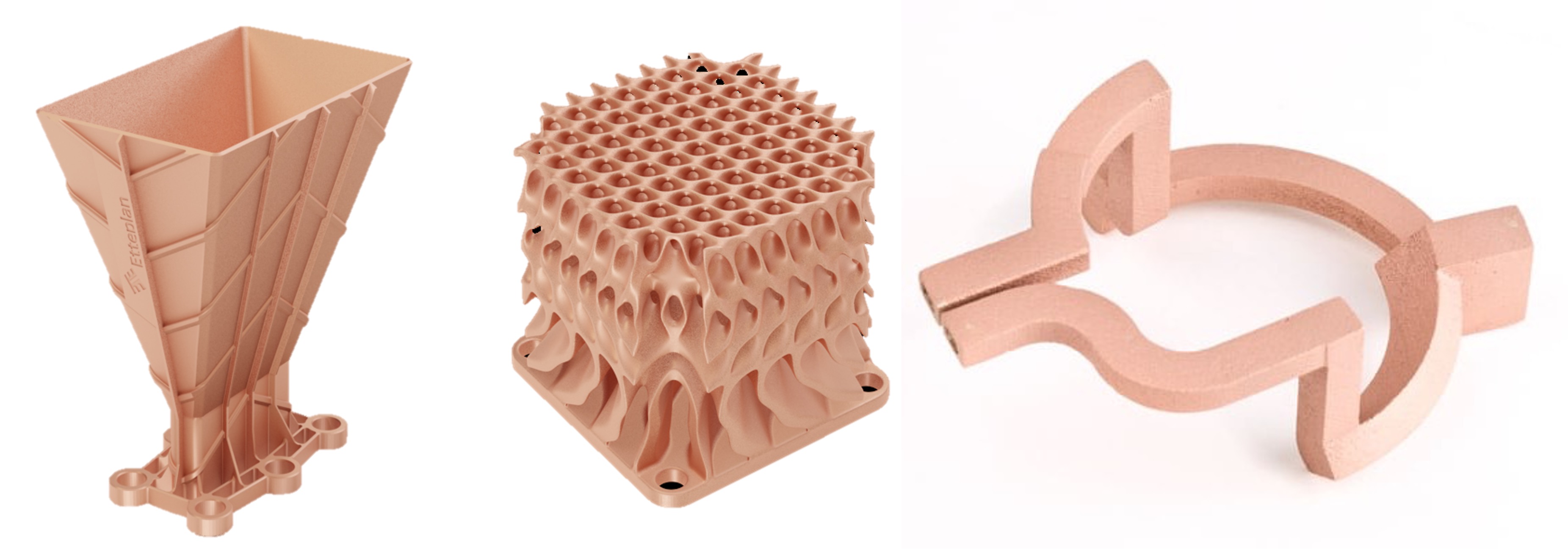
Copper 3D printing has the capability to create highly complex shares, internal geometries, lattice structures, and tiny features which are impossible to get by conventional manufacturing means. Copper 3D printing has the potential to unlock innovation and performance realization which wasn't possible due to the limitations of conventional manufacturing. Topology-optimized design reduces weight, and product complexity and lowers the overall costs and manufacturing lead time. The design which requires a manufacturing lead time of weeks could be created in a matter of hours substantially reducing the time to market.
Cover images source: Markforged(Digital Metal), GH Induction
Blog created by - 3D SculpLab Team