Introduction
Micro 3D printing or µAM is the process of creating the part with very small features measuring in microns. Current available commercial machines create parts with resolution max up to 25~30 microns. However, the µAM machines provide resolutions of less than 5 microns. Few specialized AM technologies create incredibly tiny parts in nanometers that is 1000 times smaller than micron size. The expanding requirements for microfabricated parts across a wide spectrum of industry such as medical, electronics, automotive etc. has led to the accelerated development of micro-AM technologies. Micro AM creates parts and shapes so tiny in nature that cannot be made by the conventional manufacturing set-up.
There are some specialized conventional manufacturing technologies (micro injection molding) available that can make parts at microscale but not widely available due to high costs & complexity and expertise available with very few companies. On the other hand, µAM provides a viable and cost-effective option to companies to manufacture prototypes and parts at micro/nanoscale from one to a few thousand in the shortest possible time. Currently, most µAM parts are made by resin-based SLA process means photopolymerization by exposing the resin to light. Few companies have developed the capability of making micro-AM parts in metals such as aluminum, copper, steel etc. At present, µAM is a relatively new development and acts as an additional option w.r.t current AM technologies.
Micro AM Technologies
- Micro SLS
- Micro SLA
- Projection MicroStereolithography (PµSL)
- Two-photon polymerization (TPP)
- Lithography-based Metal Manufacturing (LMM)
- Electrochemical deposition
- Nano ink-jetting
Micro SLS
It is the same as typical powder bed fusion technology where a high-intensity laser beam scan in 2D format across the powder bed layer by layer creates the final shape. µSLS usually refer to the metal SLS process. The powder particle size is much smaller than the standard SLS and ultra-thin laser beam ultimately creates the part with very high surface detail with sub 5micron resolution and build speed of more than 60mm3/hr.
In this process, a layer of metal nanoparticle ink is first overlayed onto a substrate and then dried to produce a consistent layer. Then a precise positioning system locates the substrate under the laser scanning system. The laser scanning system scans the laser light across the length and width of the substrate and the digital micromirror array is used to heat and sinter the nanoparticles into the required patterns. This process is repeated to get the final 3D shape.
µSLS merges the benefits of SLM AM and the micromachining process permitting the creation of parts with unbelievable details and accuracy. This process also offers very high dimensional accuracy, incredible resolution and surface finish. Complex internal cavities and channels could be easily created even the complicated assemblies could be created in µSLS.


µSLS made flow channel & other parts. Photo credits: 3D MicroPrint
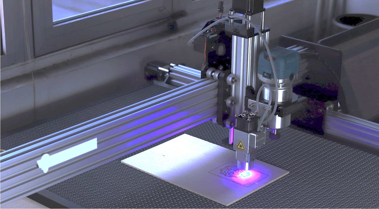
Micro SLA
This process is the same as general stereolithography which involves the polymerization of photo resin by a light source in a vat. However, µSLA is a modified version of other commercially available SLA machines to make micro-SLA parts. The modification involves the specially designed lenses which emit incredibly small diameter laser beams creating very small size cure resin parts. Also, special resins are developed for µSLA.
Projection MicroStereolithography (PµSL)
PµSL is another high potential additive manufacturing process due to its low cost, speed and accuracy. Also, a wide range of materials such as ceramics, polymers and biomaterials with applications ranging from micro-opticals, metamaterials, micro fluids, tissue engineering and micro biomedical devices. PµSL uses a projector to project the entire 2D cross-section onto the surface which cures the liquid layer in one go. The process is repeated to generate a 3D part. PµSL works on DLP (Digital Light Processing) principal which share commonality with other commercially available DLP printers. This process was able to achieve a layer thickness of 1µm.

PµSL made 5µm turbine. Photo credits: BMF3D

PµSL made Micro medical device. Photo credits: BMF3D
Two-photon polymerization (TPP)
TPP or 2PP is perhaps the most precise AM technology to create nanoscale complex shapes and structures. This used a highly focused Femto scale laser along with scanning mirrors. 2 photons are absorbed by the photo resin initiating the local polymerisation process to create a solid element known as a voxel. The process is repeated layer by layer to generate a 3D part. Applications are in the field of material engineering, microdevices etc.
Lithography-based Metal Manufacturing (LMM)
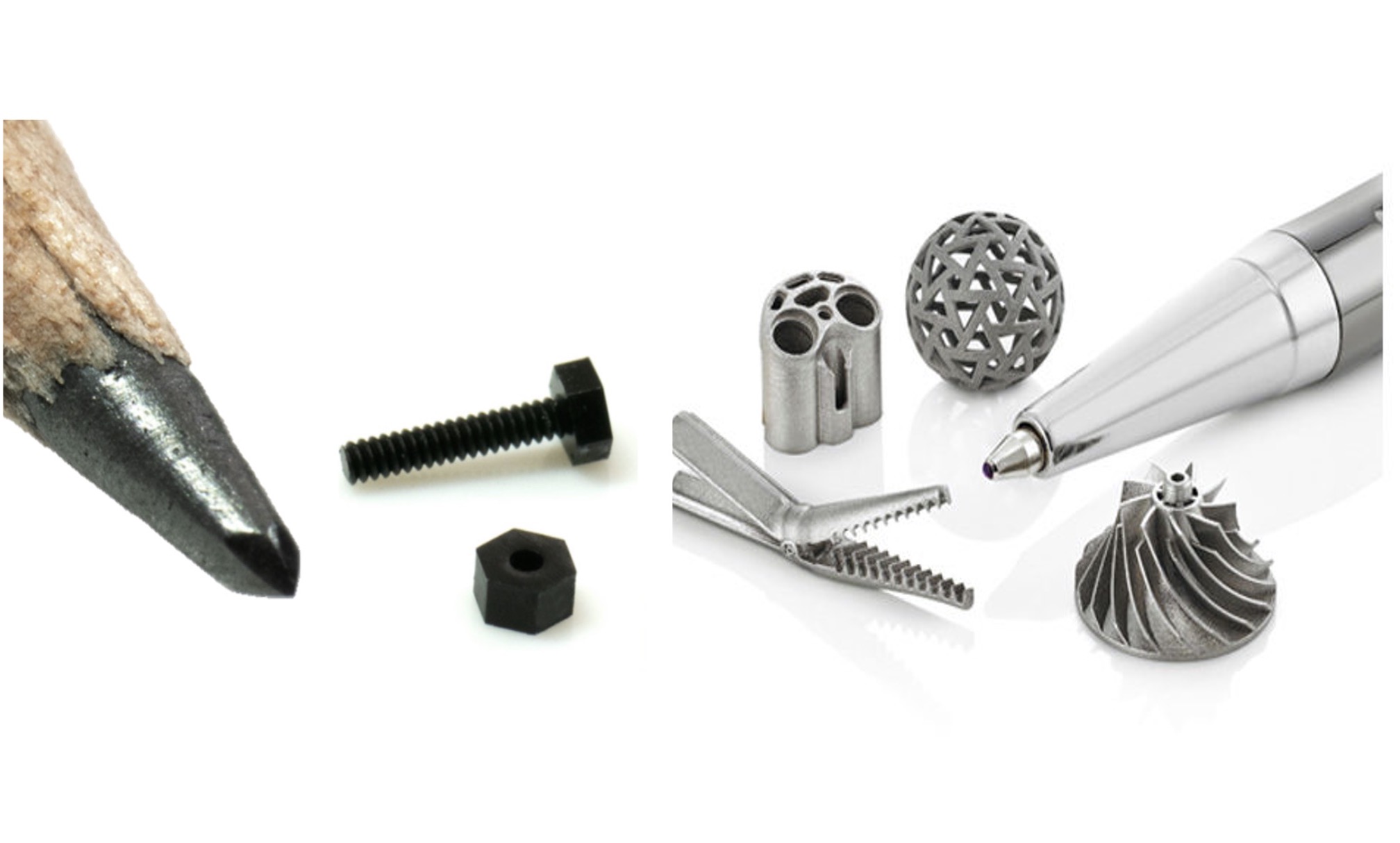
In this process, the tiny metal particles are suspended in a photosensitive resin-based solution up to 50% of the total volume and then cured by a light source layer by layer creating a ‘green part’. The curing process is very similar to any other vat polymerisation process. Later, the green part is sintered inside a furnace to obtain the final shape. The sintering process is like the MIM process (Metal Injection Molding). This process can create highly complex metal structures with good dimensional accuracy and low surface roughness. Available materials are stainless steel, titanium, brass, copper etc.

LMM made part. Photo credits: Incus3D
Electrochemical deposition
This is another very versatile µAM technology developed by Exaddon in which an iontip is suspended into an electrolytic bath with metal ions. The liquid is passed thru a micro-channel that is precisely controlled by air pressure. At the end of the micro-channel, the metal ions are electro-deposited onto the print surface creating solid metal atoms. Deposited metals atoms are combined into making solid elements called voxels. The printed part can be used immediately without any post-processing.
Nano ink-jetting
Nano ink-jetting works like deposition solid suspension or liquid material on to surface thru a nozzle within the print head. The print head moves in a 2D layout generating the layer. The deposited ink is cured by exposure to a light source (UV or infrared) to create a solid layer. The curing system is integrated within the print head. With each pass, the ink is deposited and cured simultaneously. The key parameter in an inkjet printer is the nozzle opening and droplet size which affects the layer resolution. Smaller the nozzle size higher the part resolution. This AM process is suitable for making a complex layout PCBs with a conductive ink material in liquid form. Once printed, the part does not need any post-processing and could be used immediately.
Applications of micro 3D Printing
Electronics industry
Micro 3D printed electronics and semiconductors can greatly improve the performance & functionality of the final product such as PCB’s, embedded circuits, electromagnets, molded Devices, antennas, sensors etc. If applied for mass production, will hugely simplify the supply chain by directly printing circuits in house manufacturing. Micro 3D printing will also overcome the difficulty faced by the engineers in fabrication and testing microelectronic circuits.

Microscale electronic part for 5G application. Photo credits: Exaddon
Medical industry
The medical field can greatly benefit from µAM in terms of miniaturization of medical devices (stents, pacemakers) and medical research. µAM could be used to make medicine delivery devices and microrobots for applications like microneedle and robotics sensors providing real-time feedback from generally inaccessible parts of the human body.

Micro 3D printed needle. Photo credits: University of North Carolina
Automobile & Aerospace
Microelectronics could greatly simplify the over design and architecture of the electronic devices especially in sensors design monitoring pressure, temperature, current, humidity, vibration etc. The overall benefit would be greatly enhancing the performance, design simplification, ease of the supply chain.
Microfluidics
Microfluid engineering studies fluid flow behaviour across tiny flow channels when the flow is manipulated. Its application ranges from inkjet printing, micro heat exchangers for microcircuits. µAM could be leveraged to create channels, structures and prototypes in a cost-effective manner from a single unit to limited mass production.
Micro-optics
µAM could enable the development of tiny size lenses, micro prisms and other optical objects measuring in microns. Potential applications in the field of telecommunication, medical, processing equipment and consumer electronics.
Advantages of µAM
- µAM costs are lower than conventional manufacturing techniques for microfabrication. It is very expensive to make microfabrication thru micro CNC or micro injection molding. Very few companies have that expertise in making micro parts thru conventional manufacturing.
- µAM delivers parts/prototypes at a greater speed than microfabrication thru conventional manufacturing enabling the designer to iterate design at a faster rate.
- Complex shapes including the entire assemblies could be produced at once, hence, greatly simplifying the entire production process.
Drawbacks of µAM
- Limited material option available. Currently, µAM is mostly available with polymers. Metal µAM is still under development
- Higher costs for high quality.
Conclusion
Advancements in micro printing will unravel new frontiers for µAM such as tiny size components for wearables, micro tooling’s, embedded electronics, lightweight components etc. Increased print resolution along with additional material options are a few of the points which will drive further development of µAM.
Blog created by - 3D SculpLab Team